Daedalean Tensor Accelerator: Achieving the Theoretical Maximum Speed Rating
Applications based on AI/ML and processing computer vision are computationally demanding on a level that is unprecedented in avionics. Here’s the story of the challenges we face with our use cases and how we address them.
What Was the Goal
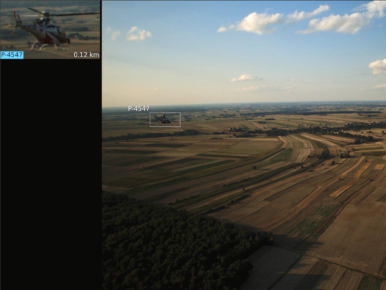
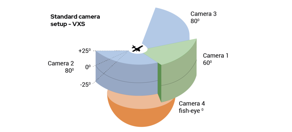
Daedalean’s Visual Awareness System (VXS) relies on the input from several (one to four) cameras installed on an aircraft.
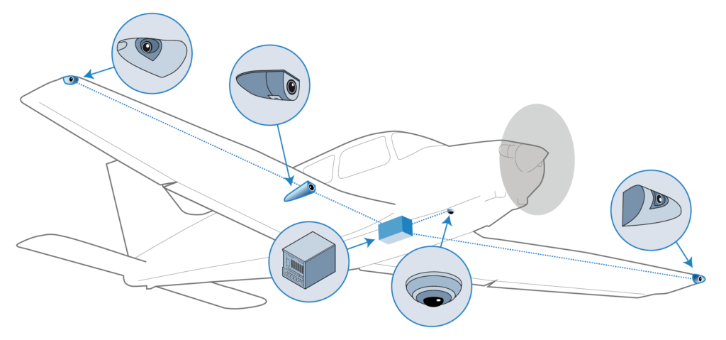
The input from the forward- and sideways-looking cameras is used by the traffic detection and landing guidance components of Daedalean’s system. The fisheye camera, facing downwards, provides input for the positioning and vertical landing guidance components.
The stream from each camera is directed to a computing platform (VXP) and processed by Convolutional Neural Networks (CNN) to detect air hazards and runways, allowing the technology to serve as another pair of eyes in the cockpit. The acquired data – coordinates, velocities, angles – are then sent to the pilot display or to the autopilot.
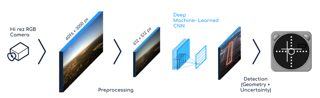
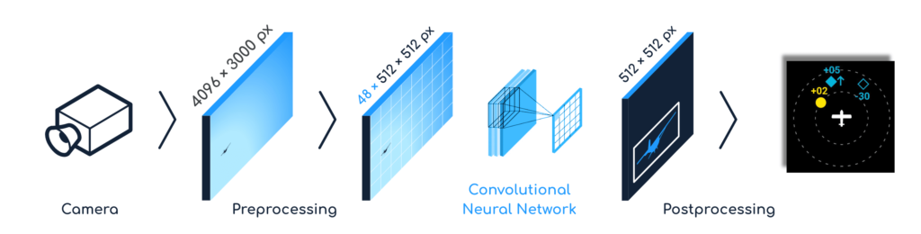
What does this mean in terms of performance? To reliably recognize aircraft and runways in real time, Daedalean’s applications require six frames per second (fps) of 12 Megapixels each. To process this amount of data, they need a minimum of one trillion (10^12) operations per second or 1 TeraOPS (TOPS) per camera. Therefore, to handle four camera streams, the Visual Awareness System needs to process 288 Megapixels per second, and a minimum computational power of four TOPS is necessary.
The top-performing option in the aerospace industry was, until recently, the venerable PowerPC architecture. Initially designed in the 1990s, the last version on the market that was certifiable for use in avionics featured four cores with a maximum clock speed of 1.6 GHz (and you had to disable three out of the four cores to meet the determinism requirements the aviation certification demands). For high-performance tensor computations, such as those used in Daedalean’s applications, the only available GPUs for use in avionics were the AMD Radeon 8860 and 9170. Together, this setup would barely support a single camera stream.
What Was the Solution
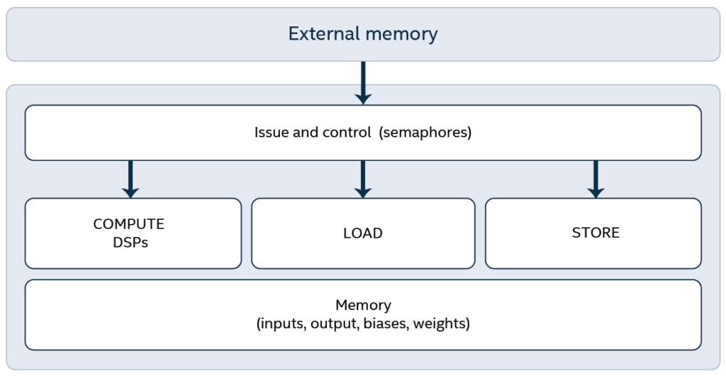
We required an airworthy computing platform as the base of the VXS that could provide a minimum of four TOPS to handle the necessary computations in real-time. We created the Daedalean AI Accelerator (DAIA) card powered by an FPGA, field-programmable gate array. The heart of the card forms our specially designed computing platform, which we named Daedalean Tensor Accelerator (DTA).
The initial version of the DTA was inspired by Versatile Tensor Accelerator, an open source deep learning computing platform. During its first demo, mid-2022, the DTA was able to process the images only at one frame per second and at the clock frequency of 100 MHz – that is, to the level that showed that the DTA worked: it could make computations, and we could put it onto the system, but it was not nearly fast enough. So the big challenge for our Platform team during the fall of 2022 was to make it work faster to process 6 fps.
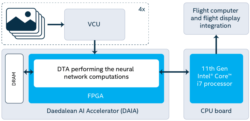
Note: Our whitepaper with Intel published last week presented the reference architecture for a highly performant computational platform capable of performing neural network computations and certifiable for use in avionics. The design was based on the 11th Gen Intel® Core™ i7 and Intel® Agilex™ F-Series FPGA. This reference architecture is based on an actual prototype we created, where another FPGA model was used – Xilinx® Kintex® Ultrascale+™.
The theoretical maximum speed rating amounts to around 575 MHz for the Xilinx implementation (Kintex UltraScale+ FPGAs Data Sheet: DC and AC Switching Characteristics (DS922), table 34). Emulations of the DTA on the Intel Agilex FPGA estimate that we will be able to achieve 670 Mhz.
In this post, we’ll delve into the inner workings of the DTA, exploring the architecture that makes achieving this level of performance possible. We’ll also discuss the trade-offs and optimizations in building a hardware accelerator that can handle our computational requirements.
How We Achieved 500 MHz for Processing 6 FPS
The DTA can be thought of as an array of lots of digital signal processing (DSP) slices (around 1800 in the case of Xilinx Kintex Ultrascale+, but in Agilex there will be many more), some internal memory, and a control unit.
The DTA architecture decouples the processes of loading data from memory, storing results, and doing the actual computations. It relies upon our internally developed custom instruction set, providing independent streams of load, store, and compute instructions. Dependency flags control the correct order of execution of the three streams at selected points in the program as determined by our compiler. This design enabled us to quickly identify the bottlenecks of our architecture at every stage of the development, concentrate our efforts on improving performance – and see the fruits of our work immediately in the next version.
Ideally, we want each DSP core to do something in every cycle at the highest possible frequency. So, we want to keep them:
- as efficient as possible (do as much work as possible per clock cycle)
- as busy as possible (to do some work at every clock cycle)
- as fast as possible (to do as many clock cycles as possible per second)
Getting to the necessary level of performance required optimizations on all levels of the design, from the compiler at the top and down to how the electrical signals run on the FPGA and how the individual components are placed on it. In the beginning, the team collected ideas (to figure out how to improve the instruction architecture of the DTA, identify bottlenecks in the actual DTA architecture, and improve the physical placement of the components of the DTA on the FPGA), then planned the collective work. Team members worked independently, focusing on different levels, and had regular meetings to align activities.
First, we needed to make sure that the DSPs were as efficient as possible.
To achieve this, we worked with our neural network architects to optimize the precision of the calculations, such that we can process two data elements in parallel per clock cycle on the built-in multipliers of the FPGA. As a consequence, we effectively double the performance of our compute instructions. (This method is well-known and outlined by Xilinx here.)
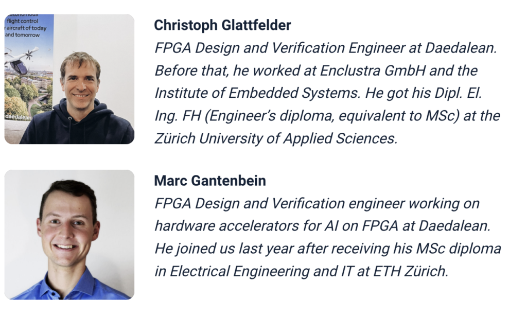
Also, to find an optimized solution that maximizes the use of the DSPs, Noam Gallmann and Johannes Frohnhofen have carefully mapped the operations required by the neural network to the capabilities of the DSPs. This work involved analyzing the mathematical operations involved in the neural network and reformulating them to take advantage of the DSP’s efficient processing capabilities. Noam and Johannes also carefully examined the interdependencies between different operations and their results to identify opportunities for optimization.

Then, we wanted the DSP cores to never have a rest and produce new results every cycle. If data is available, the cores can always run, no matter what the rest of the system is doing. Further optimizations were made to the compiler to reduce the idle time when the compute module was waiting on the load module, increasing the compute units’ utilization.
Finally, we wanted the DSP cores to work as fast as possible. This is where the most work of the Platform team was put in.
Marc Gantenbein and Noam Gallmann oversaw the improvement of the overall architecture of the DTA – optimized the individual compute units, the memory structure, and fetching instructions and data from external memory. This endeavor took lots and lots of minor incremental improvements – writing the code in a way that makes it possible to run at the required speed with as few resources as possible.
Christoph Glattfelder optimized the clocking of the design. As various parts of the FPGA work at different frequencies, the DTA needed to be partitioned into slow and fast regions to help ensure that only the essential parts of the design were optimized.
Meanwhile Dr. Sota Sawaguchi worked on the detailed placement of the computational units in the DTA (floorplanning) to help minimize the distance between storage elements and corresponding compute units in the data paths, which was also critical for increasing the frequency. Floorplanning involved giving the algorithms of the design tools hints on where to place components like the DSPs and memories to make the design as effective as possible. By bringing the storage elements as close together as possible, the team minimized the distance that data had to travel, making it possible to increase the frequency further.

After all the pain, sweat and occasional tears, the speed of processing the images from the cameras by our neural networks increased to 6.4-7 fps (depending on the specific neural network being executed) at a 500 MHz FPGA clock frequency.
It is important to note that the relationship between frequency and performance is not linear. Simply increasing the frequency to 500 MHz would not necessarily result in a proportional increase in performance due to dependencies between the modules in the architecture. Some modules may consume data faster when operating faster, leading to increased load on other components and potential stalls. However, at this stage, we were able to boost the memory bandwidth and thus maximize the interaction between the modules. Because of that, the increase from 350 to 500 MHz showed a nearly linear improvement in performance. As frequency increases further, the relationship between frequency and performance will likely level off, and additional optimizations might be needed.
Future Migration to Agilex
The current Xilinx® Kintex® Ultrascale+™ implementation can only manage one camera stream per chip. But we plan to implement the version of the platform according to the reference architecture we presented in the whitepaper mentioned above, based on the Intel® Agilex™ FPGA, so it can handle up to four camera streams on a single chip. Reducing the four DAIA cards to just one card will provide estimated SWaP improvements of more than 50%. Emulations of the DTA on the Intel® Agilex™ FPGA estimate that we can achieve 670 Mhz or at least a 24% speed-up. This frequency boost will enable us to add further capabilities to our neural networks for even better detection and tracking performance, and will allow us to use our platform in yet unexplored use cases.
This article was originally published by Daedalean.